
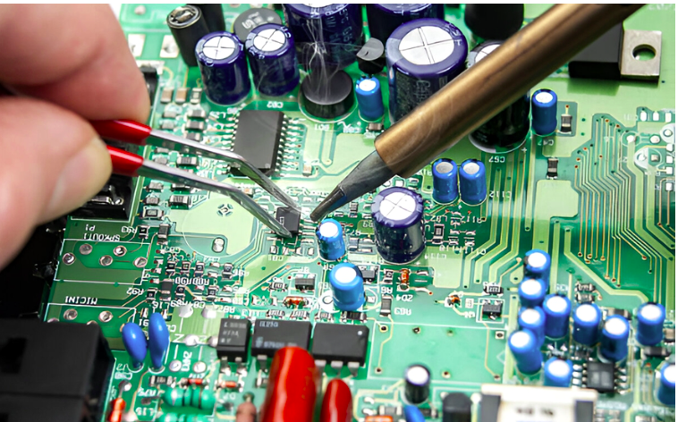
Printed circuit board assembly is one of the most critical stages in electronics manufacturing. Even
when a PCB has been designed correctly and fabricated to precise specifications, defects introduced
during assembly can affect performance, reliability, and product lifespan. As electronic devices
become more compact and complex, manufacturers must pay close attention to assembly quality to
ensure consistent results. Understanding Common PCB Assembly Defects is essential for engineers,
quality control teams, and manufacturers seeking to improve production yields and reduce costly
rework.
PCB assembly defects can occur for various reasons, including improper soldering, inaccurate
component placement, inadequate process control, material issues, or design-related challenges.
While some defects are easy to identify during inspection, others may only appear during testing or
after a product has been deployed in the field. By understanding the most common assembly
defects and their root causes, manufacturers can implement preventive measures that improve
product quality and manufacturing efficiency.
Understanding Common PCB Assembly Defects
Common PCB Assembly Defects refer to manufacturing issues that occur during the process of
mounting and soldering electronic components onto a printed circuit board. These defects can affect
electrical connectivity, mechanical stability, signal integrity, and overall product functionality.
Assembly defects may range from minor cosmetic imperfections to serious faults that cause
complete circuit failure. In high-reliability industries such as aerospace, automotive, medical devices,
and industrial automation, even small assembly defects can create significant operational risks. This
is why modern electronics manufacturers invest heavily in quality control systems, automated
inspection technologies, and process optimization techniques.
The majority of assembly defects originate from soldering processes, component placement errors,
material inconsistencies, or improper manufacturing parameters. Identifying and correcting these
issues early is essential for maintaining production quality.
Solder Bridging
One of the most frequently encountered Common PCB Assembly Defects is solder bridging. This
defect occurs when excess solder creates an unintended electrical connection between adjacent
pads, component leads, or conductive traces.
Solder bridges often develop when too much solder paste is applied during stencil printing or when
component spacing is extremely tight. Improper reflow temperature profiles can also contribute to
solder migration during the soldering process.
The presence of a solder bridge can create short circuits that prevent the PCB from functioning
correctly. In some cases, the defect may cause immediate failure, while in others it may result in
intermittent electrical issues that are difficult to diagnose.
Proper stencil design, controlled solder paste application, and optimized reflow profiles help
minimize the risk of solder bridging.
Cold Solder Joints
Cold solder joints are another common defect that can significantly affect circuit reliability. This
problem occurs when solder fails to melt and flow properly during the soldering process, resulting in
a weak electrical and mechanical connection.
A cold solder joint often appears dull, rough, or uneven rather than smooth and shiny. These joints
may initially function correctly but can fail over time due to vibration, thermal cycling, or mechanical
stress.
Common causes include insufficient heating, contaminated surfaces, poor solder quality, or incorrect
process settings. Because cold joints can create intermittent failures, they are among the most
challenging assembly defects to identify and troubleshoot.
Maintaining proper soldering temperatures and ensuring component and PCB cleanliness are
essential for preventing this issue.
Insufficient and Excessive Solder
The amount of solder applied during assembly directly affects connection quality. Insufficient solder
occurs when an inadequate quantity of solder forms the joint, resulting in weak electrical
conductivity and reduced mechanical strength.
Conversely, excessive solder creates oversized joints that may hide defects, increase the risk of
bridging, or cause reliability concerns. Both conditions can compromise product performance and
lead to premature failures.
These defects often result from improper stencil design, inaccurate solder paste deposition, or
poorly controlled soldering processes. Consistent process monitoring and regular equipment
calibration help maintain optimal solder volumes throughout production.
Tombstoning of Surface-Mount Components
Tombstoning is a defect commonly associated with small surface-mount components such as
resistors and capacitors. During the reflow process, one end of the component lifts from the PCB,
causing it to stand vertically instead of lying flat on the board.
This phenomenon occurs when uneven solder wetting forces develop during solder reflow.
Differences in pad size, thermal distribution, solder volume, or component placement can contribute
to tombstoning.
A tombstoned component typically loses electrical connectivity on one side, resulting in circuit
malfunction. Preventing this defect requires careful PCB design, balanced pad geometry, accurate
component placement, and optimized thermal profiles.
As component sizes continue to shrink, controlling tombstoning becomes increasingly important in
modern electronics manufacturing.
Component Misalignment
Accurate component placement is essential for successful PCB assembly. Component misalignment
occurs when a part is positioned incorrectly relative to its designated pads.
Even slight placement errors can affect solder joint quality and electrical performance. Severe
misalignment may result in open circuits, short circuits, or mechanical instability.
Several factors can contribute to this defect, including inaccurate pick-and-place programming,
machine calibration issues, improper component handling, or PCB dimensional inconsistencies.
Modern automated placement systems provide exceptional accuracy, but ongoing equipment
maintenance and process verification remain necessary to minimize placement-related defects.
Open Circuits and Missing Components
Open circuits occur when an electrical connection is incomplete, preventing current from flowing
through the intended path. Missing components represent a related assembly issue where required
parts are not installed during production.
These defects may result from feeder errors, component shortages, machine malfunctions, or
process oversight. Open circuits can also develop due to poor solder joints or damaged PCB traces.
Because these issues directly impact circuit functionality, they are typically detected during electrical
testing procedures. Automated Optical Inspection and In-Circuit Testing systems help identify
missing components and connectivity problems before products proceed to final assembly stages.
Voids in Solder Joints
Voids are trapped pockets of gas or air that form within solder joints during the reflow process.
Although some level of voiding is generally acceptable, excessive voids can reduce thermal
conductivity and mechanical strength.
This defect is particularly concerning in power electronics, automotive systems, and high-
performance applications where effective heat dissipation is critical. Large voids may lead to
localized overheating and long-term reliability problems.
Voiding can result from moisture contamination, volatile materials in solder paste, or improper
thermal profiles. Manufacturers often use X-ray inspection systems to evaluate void levels in critical
solder joints.
Careful material selection and process optimization help reduce void formation.
Inspection Methods for Detecting PCB Assembly Defects
Preventing Common PCB Assembly Defects requires comprehensive inspection and testing
throughout the manufacturing process. Modern electronics manufacturers rely on multiple quality
control technologies to identify defects before products reach customers.
Automated Optical Inspection systems use high-resolution imaging to evaluate component
placement, polarity, solder quality, and assembly accuracy. These systems can rapidly inspect large
quantities of boards while maintaining consistent quality standards.
X-ray inspection is essential for examining hidden solder joints beneath Ball Grid Arrays and other
advanced semiconductor packages. It allows manufacturers to detect voids, bridging, insufficient
solder, and other defects that may not be visible through standard visual inspection.
Functional testing and In-Circuit Testing provide additional verification by confirming that the
assembled PCB operates according to design specifications.
Preventing Common PCB Assembly Defects
Reducing assembly defects begins with strong process control and continuous improvement.
Manufacturers must carefully monitor solder paste application, component placement accuracy,
soldering temperatures, and inspection results throughout production.
Employee training also plays an important role in defect prevention. Skilled operators and
technicians are better equipped to identify potential issues and maintain process consistency.
Design for Manufacturability reviews can further reduce defect rates by identifying assembly
challenges before production begins. Simplified layouts, optimized pad geometries, and appropriate
component spacing improve manufacturability and reduce the likelihood of defects.
A proactive approach to quality management helps manufacturers achieve higher yields, lower
production costs, and improved product reliability.
Conclusion
Understanding Common PCB Assembly Defects is essential for maintaining quality and reliability in
electronics manufacturing. Defects such as solder bridging, cold solder joints, tombstoning,
component misalignment, open circuits, and solder voids can significantly impact product
performance if not properly controlled. Through advanced inspection technologies, optimized
manufacturing processes, skilled personnel, and continuous quality improvement initiatives,
manufacturers can minimize defects and improve production yields. As electronic products become
increasingly complex, preventing assembly issues requires close collaboration between engineering
and manufacturing teams. A strong focus on PCB Design and Assembly Company helps ensure that
products meet performance expectations while achieving long-term reliability and manufacturing
efficiency.